![]()
![]()
![]()
![]()
![]()
|
Keys to an increased understanding of the properties of new materials are embedded in their structures, ranging from the mesoscale down to the atomic level. Our research circles around electron microscopy, electron diffraction and its applications on structural characterization of materials. Our main research interest comprises three electron microscopy methods: - STEM and HRTEM imaging |
|
STEM and HRTEM imaging
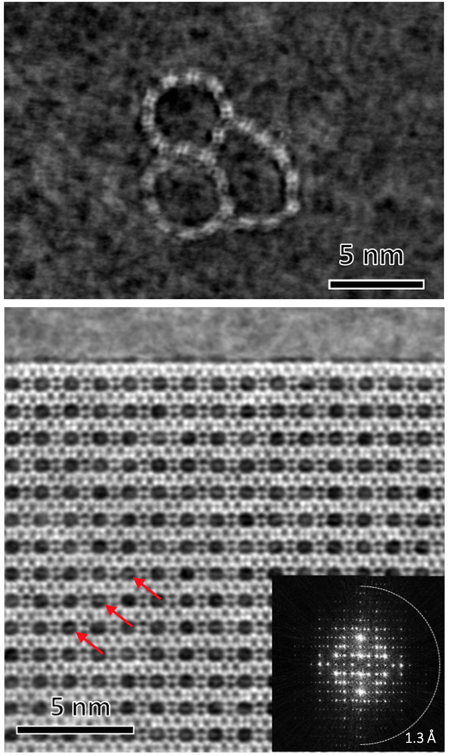
Important information for structural analysis can be gained using real space imaging methods. High-resolution TEM and STEM imaging is a versatile tool for studies of structural information down to atomic resolution. We are exploring methods such as ADF/iDPC-STEM and HRTEM, where different techniques provide various information and are suitable for different types of specimens. Imaging are important for studies of materials lacking perfect three-dimensional periodicity, e.g. materials containing disorder and defects, semi-crystalline materials or low-dimensional materials such as layered or tubular structures. Science 2022, 375, 6576, 62-66 |
 |
 |
Scanning Electron Diffraction
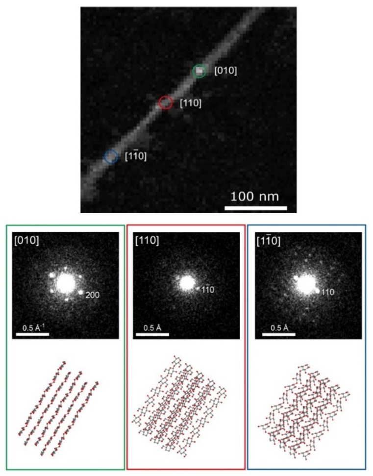
Scanning electron diffraction (SED) is an emerging method following developments in electron optics and fast and sensitive detectors. A map of the crystalline microstructure can be built up by scanning a small electron probe, 1-5 nm in diameter, in a raster across the sample and acquire 2D electron diffraction patterns from each raster point. As the sample is exposed to the electron beam for just ~1 ms, information regarding the crystal structure can be preserved even for highly electron beam-sensitive specimens. Based on the SED data it is possible to obtain information about the local crystallographic ordering at the nanoscale. This is especially interesting for materials which are very beam sensitive and are difficult to study by imaging. One such example is cellulose nanofibers where the crystalline ordering of the glucan chains can be studied. ACS Nano 2021, 15, 2, 2730-2737 |
|
Three-Dimensional Electron Diffraction
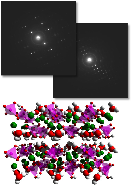
Three-dimensional electron diffraction (3D-ED) is a technique for obtaining single-crystal diffraction data from sub-micrometer-sized crystals using electron diffraction. This method has shown to be important in order to determine the crystal structure of materials that are challenging to grow large single-crystals or materials designed at the nano-scale for designated devices. Nature Communications 2020, 11 (1), 1-8 |
 |